
Talk:Operational amplifier
|
|
| Contents |
Common configurations list
I added some links which describe the basic opamp configurations. I am thinking of including them in the article itself, along with diagrams, equations for gain, input impedance, etc. but i am not sure if that will be too in depth for a wikipedia article. I am not talking about a huge article with detailed derivations of each equation, just a listing of configurations and naked equations to be used as a reference. There are a lot of sites that have this, but none have all of the information for all of the main configurations in one place, and most have derivations, or are school sites with homework problems and not the actual solutions. Should I undertake this or just leave the links? - Omegatron 19:29, Feb 18, 2004 (UTC)
Perhaps I will make an article Standard operational amplifier configurations and link it from here. - Omegatron 17:03, Feb 27, 2004 (UTC)
I would like some opinions, please. I am making a list of the common configurations, to be used as a reference, and I don't know if I should put it here or make a new article for it, since it is somewhat detailed and long. It is on my user page for now, incomplete. I guess I will stick it in this article if no one says anything. - Omegatron 14:40, Mar 23, 2004 (UTC)
- I think it would be good to eventually have a separate article on each common configuration, with a very basic description in the main article. Many of these op-amp circuits are widely enough used to be the basis for encyclopedic, albeit somewhat technical, articles. CyborgTosser
- Well, theoretically, one of the things WP is not is a textbook, so I didn't want to go too in depth about it, and just make a list that could serve as a reference. (When i go to look for this stuff online i invariably find homework assignments that just want me to re-figure it out myself.) But I guess we could for the very common ones. - Omegatron
Probably no one cares, but there are two different versions of the common configurations section, different only in formatting, at User:Omegatron/opamps. Which is better? - Omegatron 18:09, Jun 14, 2004 (UTC)
New graphics/notation
I think it would look better if the voltages were labeled with subscripts and +/- as follows:
Original:
Missing image
Opamp.png
opamp
vo = (-K * vo) + vp
vo = 1/(1+K) * vp
New:

Vout = (-K * Vout) + V+
Vout = 1/(1+K) * V+
Does anyone like the original graphic and voltage notation better? Omegatron 18:57, Feb 27, 2004 (UTC)
- I ended up just being bold and changing this. - Omegatron 14:40, Mar 23, 2004 (UTC)
- I think the new version is much improved. Very good for a web page, really. --blades 23:40, Mar 24, 2004 (UTC)
Op-amp internals
A really elementary question - how would one build a op amp out of transistors, resistors, etc? All the descriptive material seems kind of black-boxy to me. Stan 19:41, 22 Mar 2004 (UTC)
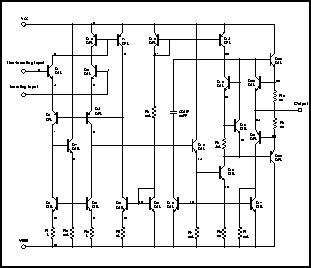
- There are a lot of different designs. We could cover the basic stages, at least. I believe it is a differential amp followed by a high gain amp followed by a unity gain power amp. I could definitely be wrong. I believe that the individual stages can be of several different types, FET vs BJT inputs, for instance. Also there are many additions in modern op-amps to make them easier to use, like short circuit protection. Here is the first schematic I found on google, to illustrate the complexity:
- - Omegatron 22:28, Mar 22, 2004 (UTC)
- Ooh, my EE knowledge paging back in, makes me feel twenty years younger... So maybe a block diagram of the amps, plus one transistor-level schematic as an example of why black-boxing it is good. :-) (Also helps explain why they were less popular before the days of ICs...) Stan 22:38, 22 Mar 2004 (UTC)
- Yes. Block diagram is good. And yes, they are complicated. Originally they were made with tubes! I'm glad I'm such a young'n, and never had to deal with such things. :-)
- Hmm. Can we use a transistor level diagram from a datasheet or is it copyrighted? http://www.national.com/ds/LM/LM741.pdf (page 4) 741 is pretty standard and relatively simple. Maybe this one? - Omegatron 22:52, Mar 22, 2004 (UTC)
- I would think they'd be copyrighted, and when WP is world-famous, National will notice... It would be OK to make one's own schematic of the 741 using their datasheet as a source; a bonus is that you can make it large and thumbnail it in the article, so we end up with something more readable than the usual muddy datasheet blob. Alternatively, one could always write to a manufacturer and ask them to donate a schematic; free publicity for them. It might be fun to write to several with a single message so that each can see the cc's to the other, get a little competitiveness going... Stan 13:09, 24 Mar 2004 (UTC)
- The thing is that these amplifiers are standards. Every company makes a 741 and probably most of them are exactly the same. But yeah, it would be really easy to make a klunky schematic version and avoid any trouble. I will do it, but it will take me a few days to get around to it. - Omegatron 17:09, Mar 24, 2004 (UTC)
- Done.

- Anything else I should add? We should outline the different sections in colored dashed lines and labels. Someone please double check it. Most probable mistakes are NPN/PNP and wiring mistakes (especially crossing wires vs 4 way junction), but I think it is right. - Omegatron 14:36, Mar 25, 2004 (UTC)
- Cool! Functional blocks shown with solid rectangles of light colors would make it perfect. Stan 17:11, 25 Mar 2004 (UTC)
Note to self: http://www.national.com/appinfo/amps/files/Opamp_Trivia_WEBCAST_FINAL.pdf page 47. ;-)
Or I could color code the circuitry itself, similar to their highlighting specific parts in dark black. Would this be easier to read? Do we have to worry about color blindness (we would have to with dashed outlines too) (i think we would just have to avoid certain colors next to each other?)
Missing image
Coloredcircuittestcases.png
Image:coloredcircuittestcases.png
- Omegatron 20:06, Mar 25, 2004 (UTC)
Alright. I did what I could:
Missing image
Opamptransistorlevelcolored.png
Image:opamptransistorlevelcolored.png
I don't know everything. Specifically the magenta section. Is it part of the lowpass filter? And what does that extra transistor on the output do? I can alter the image if some of the sections should be a little different. Please add what you know to the internals section. - Omegatron 17:06, Jul 17, 2004 (UTC)
The Magenta Section
I think that in both cases we have constant-current controllers.
Take the transistor in the output section that has a 25Ω resistor between its legs: If the bias current through the 25Ω were to increase for some reason, its base-emitter voltage would rise above, say 0.6V, the transistor would turn on more and so it would draw more collector current - out of the main output transistor's base. This would turn that off a bit and thereby reduce the bias current again.
The three transistors in the magenta section are in the same configuration except that two of them seem to form a kind of 'toned-down' darlington pair (toned down by the 50k, which reduces their combined forward gain slightly). The third one 'saps away' base current out of the first of the pair until a happy 0.6-0.7V appears across the 50Ω resistor. This sets the bias current in the green driver stage.
Any help?
Nigelj 15:43, 28 Aug 2004 (UTC)
Offset Null Adjustment
Having a bit of trouble using the offset null on the 741 amp. Is it possible for someone to walk me through it? Thanks
It's important to use the Offset Null adjustment correctly in order to get the best out of any op-amp that has one. Setting it up correctly will optimise two aspects of performance:
Offset Drift
The dc output voltage of a real op amp for any given input conditions will drift with both temperature and ageing. Correctly setting the offset null adjustment will help to minimise this in both cases.
Common-Mode Rejection Ratio (CMRR)
The dc output voltage of an ideal op-amp would be zero when the two input voltages were at the same voltage, no matter what that voltage was. In practice, there will be some change in output as the voltage of the two inputs is varied, even though they remain tied together. The ability of the amp to reject these 'common-mode' inputs will also be optimised by correctly nulling the input offset
Setting up the 741
(What follows applies to the standard μA741 of days of yore. Look up the manufacturer's data sheet for whatever amp you're using and follow the correct recommendations!)
Connect a 10kΩ linear pot between pins 1 and 5, and connect its wiper to the negative supply at pin 4. Connect both inputs (pins 2 and 3) to 0V. Note, these are the actual op-amp inputs NOT the inputs you are going to expose to the outside world, the other side of whatever input resistors. Adjust the pot until there is no voltage between pin 6 and 0V.
Important Note
Regarding the note in the the previous paragraph, it is often necessary to design in another 'zero' adjustment, which may inject a small +/- voltage into a summing junction at one of the inputs. It is important then that the 10k input offset pot is adjusted as described above to null the op-amp's actual input offset, so as to get the performance benefits described earlier. The zero adjustment is then used to create the desired behaviour of the overall circuit, without touching the input offset adjustment again.
Nigelj 16:12, 24 Oct 2004 (UTC)
Vs+/Vs- are reversed?
The voltage supply rails are mislabeled aren't they? The top one should be Vs+, the bottom Vs-.
- Oops. Good eye. Fixed. - Omegatron 16:33, Jan 31, 2005 (UTC)hi i want to know why op-amp give -15 and +15 volt supply.
Differencing input impedance
Who knows the differential input impedance of the differencing amp?

I've been told that my original calculation was wrong by someone who is usually right, so I commented it out for now. I am skeptical and think I was right, though. - Omegatron 06:32, Mar 18, 2005 (UTC)
- These comments apply to single ended output version of the circuit:
- For a floating voltage source connected between the input terminals (a microphone for example), the resistance seen by the source is simply the sum R1 + R2.
- Excellent. That's what I had previously but a senior engineer hesitantly disagreed. I think they were just confused... - Omegatron 18:12, Apr 16, 2005 (UTC)
- What is interesting about this configuration is that the input terminals will generally have a common mode voltage present that is a function of the output voltage. In fact, for the case R1 = R2, R3 = R4, the input common mode voltage is given by Vout / 2.
- The presence of this "Vout induced" common mode voltage on the input terminals and thus the cable connecting the source to the amplifier is not desirable. I have recently shown that it is possible to find values for the four resistors such that for a specified input resistance and difference gain, the common mode gain is zero and the input common mode voltage due to Vout is zero.
- For example, a balanced 600 Ohm microphone pre-amp with a voltage gain of 20 requires the following 1% resistor values:
- R1 = 590, R2 = 14.3, R3 = 11.8k, R4 = 287
- Compare these with the 'textbook' values of:
- R1 = 300, R2 = 300, R3 = 6000, R4 = 6000
- For both sets of resistor values, the pre-amp will have a nominal 600 Ohm input resistance, a difference voltage gain of 20 and a common mode voltage gain of 0. However, the 'textbook' pre-amp will generate a common mode voltage at the input terminals that is 10 times the source voltage!
- Excellent info. Can you add it to that section of the article? - Omegatron
- I'd be happy to!
- Hmm.. Actually I'm confused about where the common-mode voltage appears. Can you describe the rest of the circuit? Where is the common-mode voltage and what is it relative to? - Omegatron 18:16, Apr 16, 2005 (UTC)
- The common mode voltage on the input terminals is defined as: (V1 + V2) / 2, the average of the two input voltages. Here's a physical picture. Connect a voltmeter between V1 and ground. Connect a second voltmeter between V2 and ground. Let's say that V1 reads 9.5V and V2 reads 10.5V. The difference voltage is: (10.5V - 9.5V) = 1V. The common mode voltage is: (10.5V + 9.5V) / 2 = 10V. In words, it is the voltage common to both input terminals.
- I'm more confused now. Isn't that what's supposed to happen? That's how the difference amplifier works. There will always be a voltage on the opamp terminals because of the R2/R4 divider. You're just minimizing it by making R4 >> R2? I know the properties of an amplifier depend on the common mode voltage, and the designer tries to minimize this, but does that apply in this case? - Omegatron 23:22, Apr 17, 2005 (UTC)
- I think the confusion may be that you are referring to the opamp input terminals (V+, V-) which, as you know, must have the same voltage at all times (virtual short) when negative feedback is present. As you correctly point out, this is a pure common mode voltage. However, in the comments above, I am referring to the common mode voltage at the input terminals of the circuit (V2, V1). The common mode voltage gain (Acm) of the circuit (not the opamp) is defined as: 2(Vout) / (V1 + V2). The CMRR of the opamp is a function of the internal circuitry. For this circuit, the Acm depends on the external resistor values, not the CMRR of the opamp! It's easy to see from your fundamental equation for Vout that Acm can be made the desirable value of zero if the following condition is met:
- (1) [(R3 + R1)R4 / (R4 + R2)R1] = R3 / R1
- Not surprisingly, the condition for the amplified difference, R1 = R2, R3 = R4, also satisfies the constraint (1) for Acm = 0. Unfortunately, this arrangement generates a voltage (with respect to ground) of Vout / 2 on both the V1 and V2 terminals. Picture this: you connect a microphone to the V2 and V1 terminals of this amplifier circuit with the 'textbook' resistor values I gave above. Let's say that the microphone produces a 100mV AC voltage ACROSS V2 and V1. If you measure the voltage with an oscilloscope from V2 to ground, you will see the original microphone signal amplified by 10.5! If you connect a second oscilloscope probe to V1, you will see the original microphone signal amplifed by 9.5 and that the two voltages are in phase. If instead, you use the resistor values I gave, you would measure the microphone signal divided by two on both V2 and V1 and that this signal is truly differential. That is, the two voltages are out of phase - just what you would expect to see coming out of the microphone when not connected to the pre-amp.
- Do you use circuit simulator software such as pSPICE or an equivalent? If so, I can send you the circuit files that I used to simulate the two circuits.
Differencing amplifier with floating output?
Missing image
Opampdifferencingnoground.png
Differencing Amplifier
- These comments apply to the floating output version of the circuit:
- It seems to me that the floating output version of the diff-amp is not, in general, a valid circuit. Connect a floating voltage source, Vin, between the input terminals. The open circuit output voltage, Vout(oc), must equal Vin. The reason is that there is no path for source current and so the voltage across every resistor in the circuit is 0V. With a load resistance connected between the output voltage terminals, the circuit cannot be solved unless Vin is exactly zero.
- If each input terminal is connected to a voltage source referenced to ground, you do have a valid circuit that contains both negative and positive feedback. This means that with the appropriate choice of resistor values, the voltage gain becomes unbounded i.e., the amp becomes unstable.
- Oops. I saw it on some website and thought "whoa! a balanced output configuration!". I guess it's too good to be true... - Omegatron 18:12, Apr 16, 2005 (UTC)
- Here it is: http://webpages.ursinus.edu/lriley/ref/circuits/node5.html - Omegatron 14:17, Apr 18, 2005 (UTC)
- I've taken a quick look at the web page above and have come to the conclusion that the end of R4 that appears to be floating in the diagram above is actually the implied common node (usually the power supply ground). To see this, look at his diagram for the voltage follower (figure 26) just above his diagram for the differential amplifier circuit in question. Note that he shows Vin and Vout referenced to a floating node (the line isn't connected to anything)!
- The only way to make any sense out of this diagram (and the others on the page) is to assume that the line representing that floating node is actually the power supply common (ground). Otherwise, there is no path for current through a load! It is conventional to assume that the voltage at the output node of the opamp is referenced to the power supply common. Thus, there should be a ground symbol connected to that floating node. Further, take a look at the very first diagram (figure 22) on the page. The author shows the negative terminal of the dependent voltage source as an external, floating connection. Where is that connection in the rest of the circuit diagrams? That terminal should be shown as an internal connection to ground, IMHO. Then, it is clear that the path for load current is through the dependent voltage source in figure 22.
- Alright. So I just invented it. I've already removed it from the article. - Omegatron
- In order to have a true balanced (differential) output, I believe that you must use two opamps with the load connected between the two output terminals. This is done all the time with stereo power amplifiers. You drive the inputs of the stereo amp with equal but opposite voltages and then connect the speaker between the two outputs of the amplifier.
- Yes, the bridged amplifier. For opamps to simulate a transformer-coupled floating output, we use the "cross-coupled" connection, right? Like so:

- I just saw that diagram, assumed it to be true, and thought "Wow, a one-opamp version of the cross-coupled output!"
- You know, you can sign your talk page posts by typing ~~~ or ~~~~ for name plus timestamp. - Omegatron 17:19, Apr 18, 2005 (UTC)
- Yes, the bridged amplifier. For opamps to simulate a transformer-coupled floating output, we use the "cross-coupled" connection, right? Like so:
- That 'cross-coupled' circuit was fun to analyze! I found that the overall voltage gain of the circuit is 2 but that interestingly, the voltage gains for Vpos and Vneg are not equal but opposite. Vpos / Vin is 1.5 while Vneg / Vin is -0.5 (an inverting attenuator!). This gain imbalance produces (you guessed it) a common mode OUTPUT voltage equal to Vin / 2. To exactly simulate a transformer-coupled floating output, the common mode output voltage should be zero which requires the voltage gains for Vpos and Vneg to be equal and opposite. You've got me thinking about this when I should be doing something else! Nonetheless, I'm going to investigate this circuit to see if there is a resistor combination that fixes this problem.
- Thanks for the tip! Alfred Centauri 19:48, 18 Apr 2005 (UTC)
- I am now suspicious that the single-ended gain figures I gave above are an artifact of the circuit simulation software. When I first solved the equations for this circuit, I came up with (Vpos - Vneg) = 2 Vin. This equation only specifies the voltage difference between Vpos and Vneg. To specify Vpos or Vneg w.r.t. ground, we need another equation but for the life of me, I can't seem to get another independent one. Although I haven't confirmed this, my belief is that the positive feedback exactly cancels the negative feedback so that we no longer have a unique solution. The circuit simulator is giving the first solution it converged to. Bottom line, it appears that all we can say is that if Vpos / Vin = Apos where 0 <= Apos <= 2, then Vneg / Vin = Aneg = -(2 - Apos). I found some mention of this circuit on the web and the impression I got is that it is a very difficult circuit to balance and to keep balanced. Doesn't surprise me a bit! Alfred Centauri 22:57, 18 Apr 2005 (UTC)
Do you have to put a voltage source between ground and one of the outputs? - Omegatron 01:38, Apr 19, 2005 (UTC)
- The interesting thing about this circuit is that the differential output voltage (Vpos - Vneg) is unaffected by putting a voltage source or a ground on one of these terminals. If you connect Vneg to ground, Vpos is simply 2 Vin. If you connect a voltage source of K Volts to Vneg, Vpos is: (2 Vin) + K. Either of these connection 'forces' Apos to become 2. Unfortunately, both of these connections defeats the intended purpose of the circuit - single-ended to balanced conversion. Alfred Centauri 02:18, 19 Apr 2005 (UTC)
Instrumentation amplifier
Missing image
Opampinstrumentation.png
Image:Opampinstrumentation.png
Is this right? Should I add any other labels? Is the Vin polarity correct? I've seen both online... I've also seen ones where R2 = R3. - Omegatron 02:02, Apr 19, 2005 (UTC)
- The polarity of Vin is fine but this circuit is inverting: Vout = -Vin(1 + 2R1 / Rgain)(R3 / R2). Setting R2 = R3 simplifies the gain formula to: Vout / Vin = Adiff = -(1 + 2R1 / Rgain). Clearly, if you define Vin with the opposite polarity, the gains become positive (non-inverting). The nice thing about this circuit is that no input common mode voltage is generated by Vout.
- I think your diagram looks great! I wouldn't change a thing. Alfred Centauri 02:44, 19 Apr 2005 (UTC)